Advanced camera technologies are used with microscopes for diagnostics in the medical and life sciences industry. The occurrence of different types of imaging artifacts is a major challenge faced in microscopic imaging.

Balaji S | e-con Systems
Advanced camera technologies are frequently used for microscopic diagnostics in the medical and life sciences industry today. The high-definition cameras enable accurate analysis of microscopic specimens, allowing error-free diagnosis.
One of the major challenges of microscopic imaging is the artifacts that occurs in the images. Imaging artifacts arise due to various factors, such as the type of sensors used in the camera, the intensity of lighting on the specimen, the process of capturing the image, etc. Some commonly occurring imaging artifacts are blooming/saturation artifacts, pixelation, temporal noise, photobleaching, compression artifacts, etc.
In this blog, we will delve into the details of blooming or saturation artifacts. Read on to learn more about what causes blooming artifacts, how to reduce or prevent the blooming artifact, and the kind of cameras/sensors that can be used to avoid blooming artifacts.
What Causes Blooming?
Blooming occurs in CCD (Charge Coupled Device) sensors under conditions in which the finite charge capacity of individual photodiodes or the maximum charge transfer capacity of the CCD is reached.
![]()
Figure 1: Saturation Capacity of Pixels
The electrons generated from photons during exposure are collected in the wells (Figure 1). The maximum limit of number of electrons a pixel can contain is determined by the full well capacity/saturation capacity. The bigger the pixel, the higher the saturation capacity. This also characterizes the sensor’s dynamic range. If the generated charge exceeds the full capacity of a pixel during the exposure time, the extra charges tend to flow to the neighboring pixels. This results in blooming.
Blooming appears as a block/smear in the image (See figure 2). Blooming is most likely to occur when the scene being captured has bright spots. At the saturation level, pixels lose their ability to accommodate additional charges. Thereby, the charges from saturated pixels leak into the neighboring pixels.
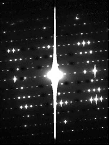
Figure 2: Blooming
How to Reduce Blooming?
Blooming can be reduced significantly by incorporating anti-blooming structures near the charge collection wells. These structures provide a safe path for excess charge removal. In high-performance sensors, a linear relationship is maintained between the photons incident on them and the output signals. A saturated pixel deviates from this linear response.
It is recommended to recognize and avoid saturation conditions rather than relying on anti-blooming techniques. Ant-blooming structures can reduce blooming to a limited extent (See figure 3).
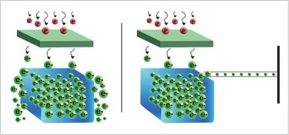
Figure 3: Anti-Blooming Drains
Using a CMOS (Complementary Metal Oxide Semiconductor) sensor instead of CCD is an ideal and the most effective alternative to prevent saturation of pixels and hence blooming.
CMOS sensor surpasses the performance of CCD sensors in the aspects of sensitivity, dynamic range, and power consumption.
The advantages of CMOS over CCD are as follows:
- Higher sensitivity from improved pixel architecture design
- Comparable noise levels
- Improved pixel well depth, which implies a higher dynamic range
- Low power consumption
- Lower cost
- Faster readout results in high frame rates
Given below is the architecture of the vertical shift register of a CCD; the pixel charge is moved down the column to be read out by the shift register. Moving a saturated pixel/charge causes overflow to the neighboring pixels. Which results in the smearing. Meanwhile, in a CMOS sensor, the charge-to-voltage conversion happens right at the pixel. The readout technology here is different. Here, the pixel voltage is digitized after activating the row and column select switches. So, there is no shifting of the charges from the pixels and no smear effect.
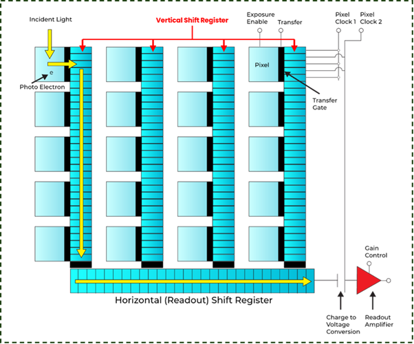
Figure 4: Internal Architecture of CCD Image Sensors
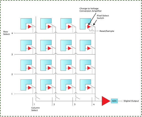
Figure 5: Internal Architecture of CMOS Image Sensors
Apart from choosing a CMOS sensor over CCD, the camera factors can be tuned as follows to avoid overexposure and reduce blooming artifacts:
- Optimizing the exposure time.
- Adjusting the gain.
- Optimizing the intensity of the illumination source.
Latest Cameras for Medical and Life Science Devices
e-con Systems, an industry pioneer, has 20+ years of experience in designing, developing, and manufacturing OEM cameras for various industries, including medical and life sciences.
Recently, we launched the e-CAM200_CUMI2020C_MOD – a 20MP, high-resolution camera based on the AR2020 image sensor from onsemi’s Hyperlux LP series. It ensures exceptional image quality, achieving a high frame rate at 20MP while seamlessly interfacing with NVIDIA® Jetson AGX Orin™, Jetson Orin™ NX, Jetson Orin Nano™, and Qualcomm® Robotics RB5. It is equipped with support for USB, GMSL and MIPI interfaces.
e-con Systems also has decades of ISP fine-tuning expertise so that the perfect image processing can be achieved on these platforms.
See all our Medical Cameras or choose the right imaging solution from our Camera Selector Page.
If you need any help in integrating the right medical camera into your device, please write to us at camerasolutions@e-consystems.com.

The content & opinions in this article are the author’s and do not necessarily represent the views of AgriTechTomorrow
Comments (0)
This post does not have any comments. Be the first to leave a comment below.
Featured Product